
2D Material Transfer Platform
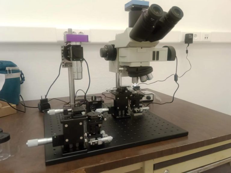
2D Material Transfer Platform is a high-precision, modular system designed for deterministic transfer of two-dimensional (2D) materials and fabrication of van der Waals (vdW) heterostructures. It enables precise pick-up and site-specific placement of graphene, transition metal dichalcogenides (TMDCs such as MoS₂ and WSe₂), hexagonal boron nitride (hBN), and other layered crystals. With sub-micron alignment, polymer-free clean interfaces, machine-vision assistance, and programmable heating, it is an ideal tool for twistronics, optoelectronic devices, and quantum-device research—from frontier fundamental labs to small-batch device prototyping.
Product Image
Core Capabilities
- Deterministic 2D Pick-and-Place
The platform supports dry transfer (PDMS/PC stamping), wet transfer (electrochemical delamination), and Pick-and-Place stacking. Users can sequentially stack multiple 2D flakes into designed heterostructures with controlled order, rotation angle, and target coordinates. - Sub-Micron Alignment
Optical positioning reaches ±0.5 μm, while an optional high-NA objective upgrades accuracy to ±100 nm. A motorized rotation stage provides ±0.1° angular control, enabling magic-angle graphene, moiré superlattices, and precisely rotated vdW stacks. - Clean, Polymer-Free Interfaces
The optimized dry-transfer process avoids polymer residue, bubbles, and wrinkles. This is critical for hBN-encapsulated devices, tunneling junctions, and low-noise quantum transports where interface contamination degrades mobility and lifetime. - Machine-Vision Flake Recognition
A built-in vision algorithm automatically detects exfoliated flake thickness and size. The user frames the target crystal in the field of view, and the system moves it to the designated coordinate with high repeatability—greatly reducing trial-and-error cost in heterostructure assembly. - Programmable Adhesion Control
An integrated heating module (room temperature to 200 °C) precisely switches the adhesion between PDMS/PC stamps and the 2D material. Controlled thermal release enables clean detachment, minimizes folds, and stabilizes the interface during multi-layer stacking. - Air-Sensitive Material Support
The system can be configured with an N₂-purge enclosure or a fully sealed glovebox version. Black phosphorus, air-unstable TMDCs, and other oxidation-sensitive materials can be transferred under continuous inert protection without performance degradation. - Micro/Nano Integration Ready
Beyond free-standing flakes, the platform aligns 2D materials onto pre-patterned electrode arrays, photonic crystals, and fabricated device structures, bridging material exfoliation with real device engineering.
Technical Specifications
| Item | Specification |
|---|---|
| Alignment accuracy | Optical positioning ±0.5 μm; optional objective ±100 nm |
| Rotation control | Motorized stage, ±0.1° |
| Transfer methods | Dry (PDMS/PC), wet (electrochemical delamination), Pick-and-Place |
| Compatible substrates | Si/SiO₂, TEM copper grid, flexible polymer, pre-patterned electrode devices |
| Microscopy | Dual-channel high-resolution microscope, coaxial epi-illumination + digital zoom |
| Environment control | Optional N₂ purge or full glovebox integration |
| Heating module | Room temperature – 200 °C, programmable adhesion control |
| Automation | Programmable multi-step transfer, real-time monitoring, parameter logging |
| Software | GUI with auto-focus, flake/layer recognition, data-log export |
| Typical materials | Graphene, MoS₂, WSe₂, hBN, black phosphorus, other layered crystals |
Typical Applications
- vdW Heterostructure Fabrication
graphene / hBN / TMDC stacks for encapsulation, tunneling, and band-engineered devices - Twistronics
magic-angle graphene, moiré superlattices, angle-dependent transport - 2D Optoelectronics
photodetectors, vdW diodes, and light-emitting 2D devices - Quantum Devices
clean-interface heterostructures for low-noise transport and confinement studies - Air-Sensitive Materials
black phosphorus and unstable TMDCs under inert atmosphere - Device Integration
2D flakes aligned to electrodes, waveguides, and photonic structures - Small-Batch Prototyping
reproducible heterostack assembly beyond manual tweezers