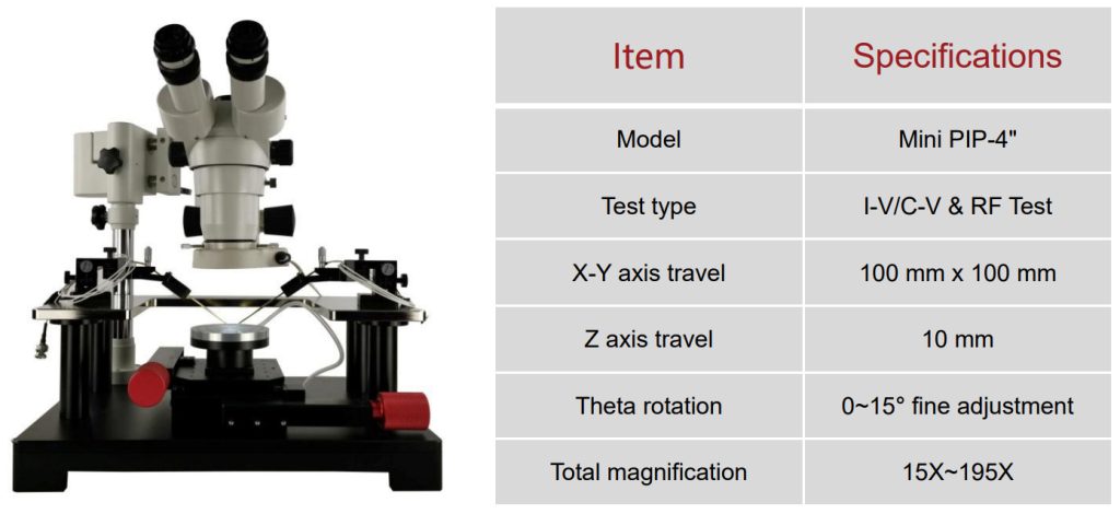
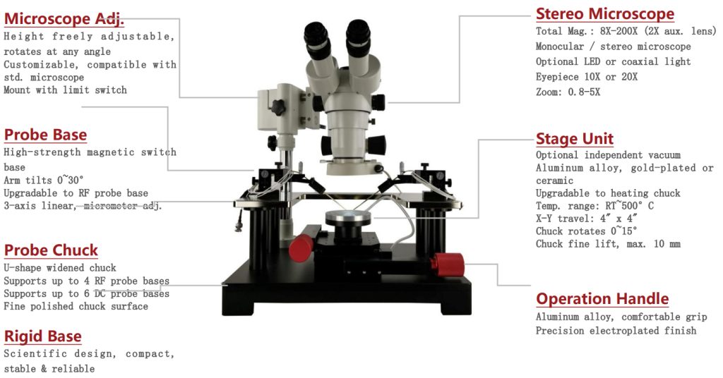
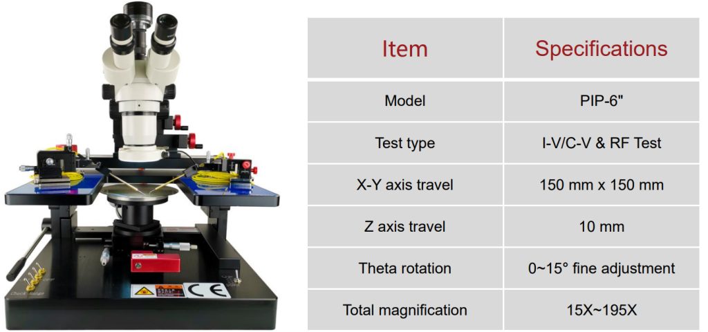
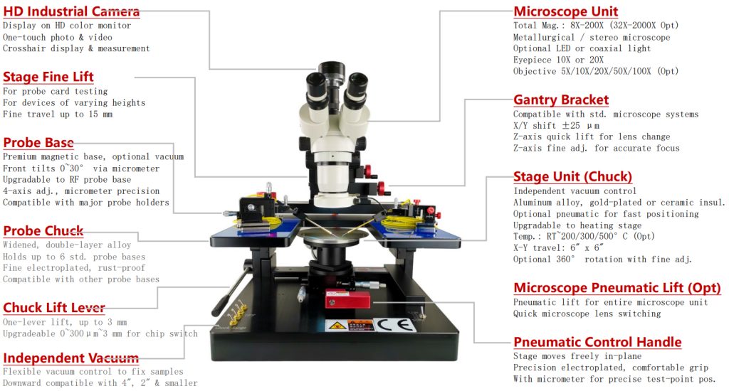
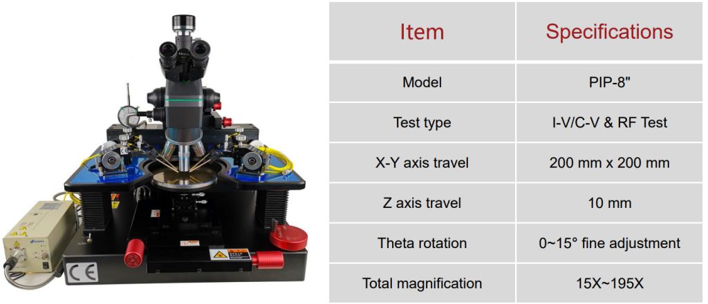
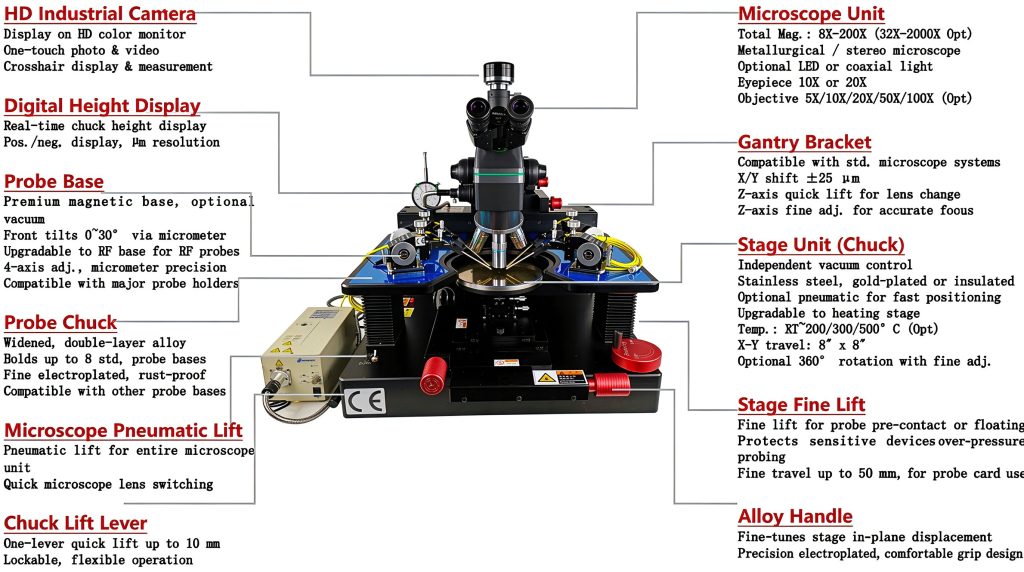
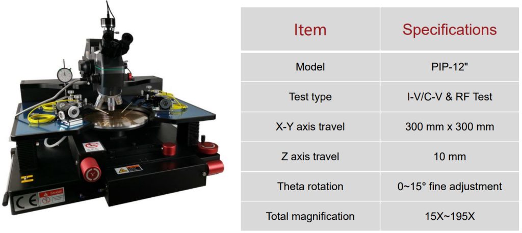
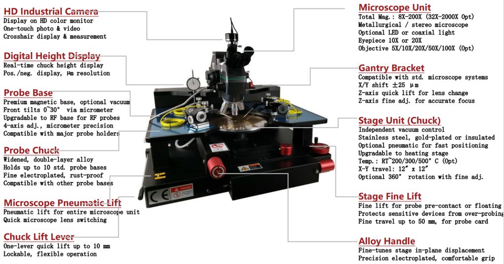

Metathermo’s PIP Series Manual Probe Stations are precision benchtop platforms for on-wafer electrical characterization of semiconductor devices, materials, and packages. Covering 4-inch (Mini), 6-inch (Compact), 8-inch (Mid-size), and 12-inch (Large) configurations, the series supports I-V/C-V testing, RF probing, and high-frequency measurements across R&D, failure analysis, and small-batch production. With modular microscope units, magnetic probe bases, vacuum chucks, optional heating stages (up to 500 °C), pneumatic controls, and HD industrial cameras, the PIP series bridges fundamental device evaluation and practical wafer-level testing.
| Item | PIP-4″ Mini | PIP-6″ Compact | PIP-8″ Mid-size | PIP-12″ Large |
|---|---|---|---|---|
| X-Y travel | 100×100 mm | 150×150 mm | 200×200 mm | 300×300 mm |
| Z travel | 10 mm | 10 mm | 10 mm | 10 mm |
| Theta rotation | 0–15° fine adj. | 0–15° fine adj. | 0–15° fine adj. | 0–15° fine adj. |
| Total magnification | 15X–195X | 15X–195X | 15X–195X | 15X–195X |
| Test type | I-V/C-V, RF | I-V/C-V, RF | I-V/C-V, RF | I-V/C-V, RF |
| Probe capacity | 4 RF + 6 DC | 6 DC (RF upgradable) | 8 DC (RF upgradable) | 10 DC (RF upgradable) |
| Chuck material | Aluminum alloy | Aluminum alloy | Stainless steel | Stainless steel |
| Heating option | RT–500 °C | RT–500 °C | RT–500 °C | RT–500 °C |
| Stage lift | 10 mm | 15 mm | 50 mm | 50 mm |
| Microscope | Stereo, 8X–200X | Stereo/Metallurgical | Stereo/Metallurgical | Stereo/Metallurgical |
| Camera | Optional HD | HD industrial | HD industrial | HD industrial |
| Pneumatic lift | — | Optional | Standard | Standard |