
3-Omega Thermal Conductivity Measurement System
The 3-Omega Thermal Conductivity Measurement System is a desktop, research-grade thermal transport platform based on the classical 3ω electrothermal coupling method. A metal micro-strip carries an AC current at frequency ω, generates Joule heating at 2ω, and produces a 3ω harmonic voltage signal that is inverted to extract thermal conductivity, thermal diffusivity, and interfacial thermal resistance of solids, liquids, films, and powders.
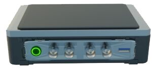
System Photo
Working Principle
Core Capabilities
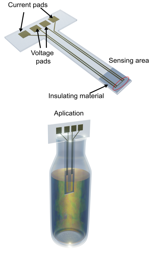
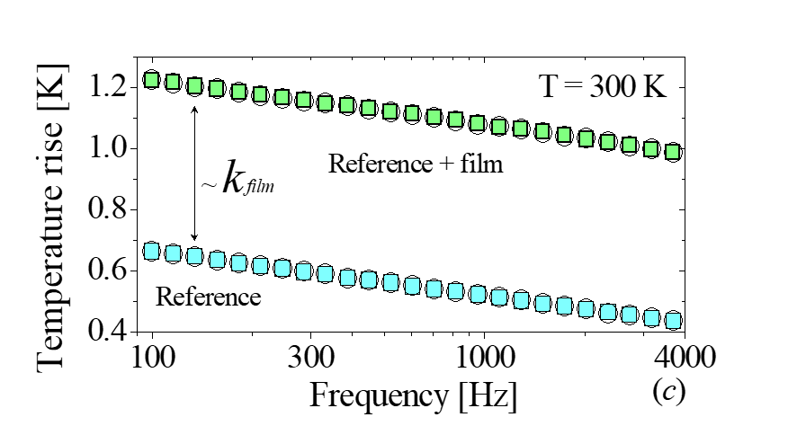
- 3ω Electrothermal Inversion Principle A metal micro-strip deposited on or embedded in the sample carries an AC current at frequency ω, producing periodic Joule heating at 2ω. The resulting temperature oscillation induces a resistance change that generates a measurable 3ω voltage component. This signal is directly inverted to obtain thermal conductivity, thermal diffusivity, and interfacial thermal resistance—without physical contact to the sample interior.
- Universal Sample Compatibility Handles solids, bulk crystals, thin films, flexible sheets, liquids, nanofluids, powders, and irregular/non-planar surfaces. Already adopted by multiple European and US laboratories for materials science, chip thermal management, thermoelectrics, and nanofluid research.
- Plug-and-Play Multi-Probe Architecture
- Solid/Flexible Probe – for bulk, thin film, and flexible sheet measurement
- Fluid/Irregular-Surface Probe – for liquids, nanofluids, powders, and non-planar samples
- 3D Transparent Detection Probe – for transparent films and micro-zone thermometry
- All probes are hot-swappable with calibrated signal conditioning
- Wide Thermal Regime & Fast Characterization Thermal conductivity range 0.1–200 W/(m·K); measurement temperature from −200 to 400 °C; typical full scan completed in ~5 minutes (single-point measurement 30–60 s). Suitable for cryogenic physics, high-temperature operation, and ambient-stable daily use.
- Optional Chip Test Stage Directly measures working temperature and thermal resistance of LEDs, OLEDs, and transistors. Supports thermoelectric co-testing of vacuum-evaporated films, 2D transferred samples, and spin-coated materials.
- Self-Developed Metrology Innovations
- Multi-view multi-frequency structured-light 3D reconstruction for specular surfaces
- 3D reconstruction, stitching, and point-cloud analysis with ±2 μm accuracy—outperforming overseas competitors (±5 μm)
- Combined capability for both precision mirror and rough-surface structured-light profiling
- Dual probe families: solid/flexible and fluid/irregular, both covering 0.1–200 W/(m·K) with <5% / <1% accuracy respectively
Key Performance Parameters
| Item | Specification |
|---|---|
| Measurement principle | 3ω harmonic electrothermal method |
| Thermal conductivity range | 0.1 – 200 W/(m·K) |
| Measurement accuracy | Solids/films: < 5%; Liquids/irregular: < 1% |
| Temperature range | −200 °C to 400 °C |
| Typical measurement time | 30–60 s per point; full scan ≈ 5 min |
| Sample types | Bulk, thin film, flexible sheet, liquid, nanofluid, powder, irregular surface, transparent film |
| Probes | Solid/flexible; fluid/irregular-surface; 3D transparent detection |
| Optional modules | Chip test stage for LED / OLED / transistor thermal resistance |
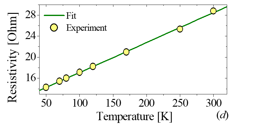
| Data output | Temperature profile, thermal conductivity–frequency curve, resistance–temperature curve |
| Communication | USB, Wi-Fi, Bluetooth |
| Power supply | 220 V |
| Host size / weight | 50 × 30 × 20 cm / ≈ 2 kg |
| Environment | Stable under humidity, temperature, and altitude variations |
Typical Applications
- Chip Thermal Management: local heating, thermal resistance, and reliability of microelectronic devices
- 2D Materials & Heterostructures: transferred flakes, encapsulated devices, dielectric/interfacial thermal resistance
- Thermoelectric Materials: thin-film thermoelectrics, Seebeck-related thermal transport
- Nanofluids & Thermal Fluids: conductivity enhancement, suspension stability studies
- Flexible & Transparent Films: OLED substrates, conductive polymers, transparent heaters
- Powders & Irregular Surfaces: catalysts, composites, non-planar engineering materials
- LED / OLED / Transistor Characterization: operating temperature and junction thermal resistance via optional chip stage