MWPS-2000

Multifunctional Wide-density Plasma System (MWPS2000)

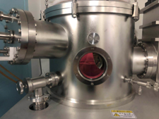
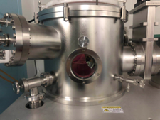
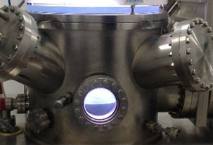
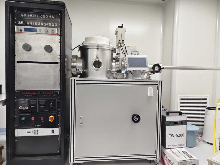
Multifunctional Wide-density Plasma System (MWPS2000)​ is independently developed by Metathermo (Suzhou) Energy Technology Co., Ltd. It is a compact, research-grade vacuum plasma processing platform that integrates the advantages of Inductively Coupled Plasma (ICP) and Capacitively Coupled Electrodeless Plasma (CCEP) glow discharge. The system achieves stable discharge across a wide density range of 10⁸–10¹³ cm⁻³. It can perform non-damaging surface modification on atomically thin layers using extremely low-density plasma, and switch to high-density mode for powerful etching and thin-film deposition assistance. It is suitable for research on new two-dimensional materials, photovoltaics, semiconductor processes, and functional coatings.

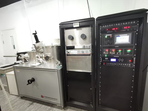
Product Image

Core Performance & Specifications

  • Plasma Density Continuously Adjustable: CCEP mode 10⁸−10⁹ cm⁻³ (electric field parallel to the substrate, weak ion bombardment, suitable for 2D material thinning/doping/cleaning); Transition region 10¹⁰−10¹¹ cm⁻³; ICP mode 10¹²−10¹³ cm⁻³ (high-density, intensive processing)
  • Discharge Architecture: Planar spiral inductive antenna (Ø410 mm × 20 mm) + Intermediate-frequency power supply (2 MHz, optional 0.5 MHz low-frequency power supply) + Matching/tuning network (20−56 nF / 1−10 nF)
  • Vacuum System: Molecular pump + mechanical pump unit, high vacuum≤5×10⁻⁴ Pa, equipped with high-vacuum gate valve and composite vacuum gauge
  • Sample Stage: Motorized rotation + lift + heating (up to 600 °C)
  • Chamber Expansion: Main chamber equipped with wide-density plasma source interface; optional 2 magnetron target positions, supporting standalone magnetron sputtering or plasma-assisted co-sputtering
  • Safety Monitoring: Multi-level detection and interlock protection for water shortage/low pressure, phase sequence, temperature, and vacuum level
  • User Experience: Human-machine interface, recipe-based process control, compact and mobile, excellent repeatability

System Composition

Vacuum Operating System
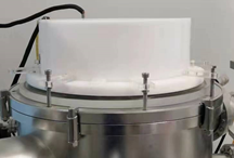
Planar Inductive Antenna
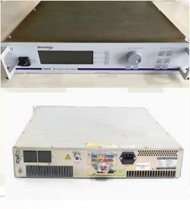
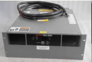
Medium-Frequency Power Source
Low-Frequency Power Source
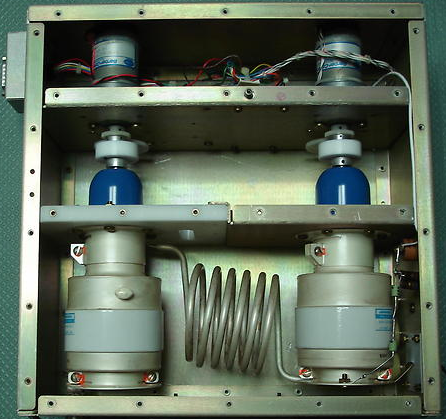
RF Matching Network

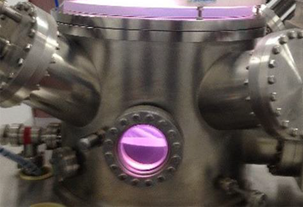
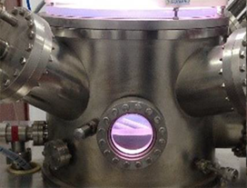
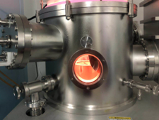
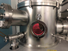
Discharge Images

ICP Mode
ne~1012-1013 cm-3
Transition Region
ne~1011 cm-3
Transition Region
ne~1010 cm-3
CCEP Mode
ne~108-109 cm-3
H2
Ar
SF6

Technical Highlights

  • Wide-Density Cross-Mode Operation
    A single system covers the full range from “near-zero ion bombardment” to “intensive ion etching,” resolving the conflict between damage-free modification of ultrathin 2D materials and high-efficiency etching required for bulk materials/hard films.
  • CCEP Parallel Electric Field Design
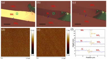
    Positive ion motion is confined to the direction parallel to the substrate, avoiding vertical bombardment. This enables layer-by-layer thinning, bandgap engineering, and surface cleaning of atomically layered materials such as MoS₂, graphene, and hBN—without membrane rupture.
  • Versatile for Research and Pilot-Scale Testing
    Equipped with a load lock, transfer mechanism, and a heated rotating stage, the system accommodates both single-piece characterization samples and small-batch pilot production. Magnetron interfaces are reserved for convenient expansion into PVD combined processes.
  • Published and Validated
    Related processes have been adopted in first-quartile publications including Nature Electronics, Nature Communications, ACS Nano, Journal of Materials Science & Technology, and Materials Science & Engineering R-Reports, covering plasma-intercalated superlattices, WO₃₋ₓ semimetal modification, layer-by-layer MoS₂ etching, crystalline silicon solar cell texturing, and more.

Typical Applications

  • 2D Materials: Layer number control, plasma-intercalated superlattices, surface doping, bandgap engineering, damage-free cleaning
  • Microelectronics / Semiconductors: SiO₂/Si₃N₄ etching, contact interface modification, pre-patterning treatment
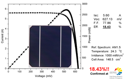
  • Energy Materials: High-efficiency crystalline silicon solar cell texturing, amorphous/microcrystalline silicon processing, silicon nitride passivation layer treatment
  • Thin Films and Coatings: Magnetron sputtering-assisted deposition, nano-scale topography construction, surface wetting/adhesion activation
  • Interdisciplinary: Chemical vapor nanomaterial growth, magnetic/metal material surface treatment, catalyst support modification

Application Examples

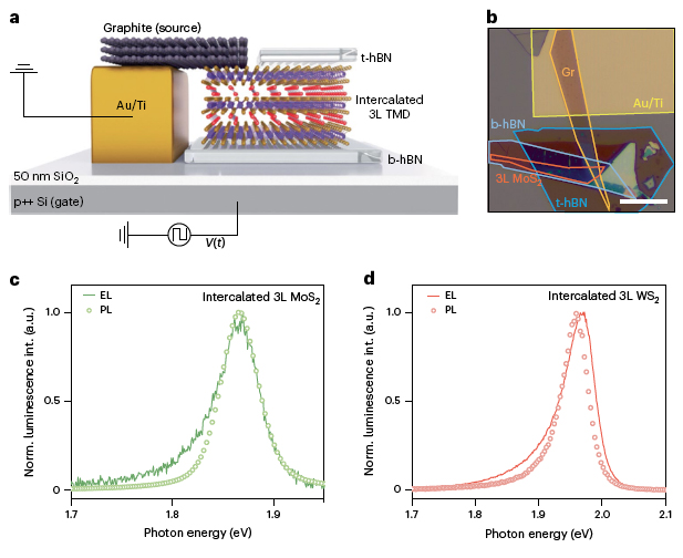
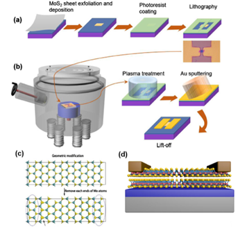
Light-emitting diodes based on plasma intercalated TMDs (Nature Electronics 2025, 8, 56)
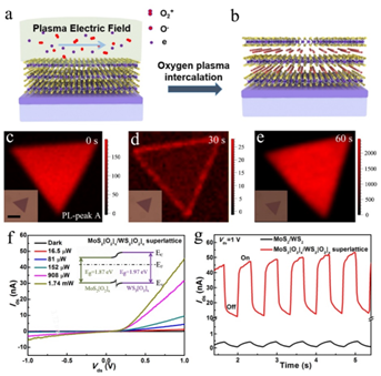
Plasma Intercalation for Constructing 2D Superlattices (Nature Communication 2020, 11, 5960)
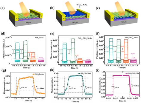
Plasma Modification of WO₃ into Semimetallic WO₃₋ₓ for Enhanced Plasmonic Photodetector Performance (Journal of Materials Science & Technology 2024, 193, 217-225 )
Plasma Etching for Enhanced Transistor Electrode Contact Performance (Journal of Materials Science & Technology 2021, 69, 15-19)
Advanced Plasma Fabrication of High-Efficiency Crystalline Silicon Solar Cells (Materials Science and Engineering R-Reports 2014, 78, 1-29 )
Layer-by-Layer Plasma Etching of Transition Metal Dichalcogenides (ACS Nano 2013, 7, 4202-4209 )

Related References

  1. Shixuan Wang, Qiang Fu, Ting Zheng, Xu Han, Hao Wang, Tao Zhou, Jing Liu, Tianqi Liu, Yuwei Zhang, Kaiqi Chen, Qixing Wang, Zhexing Duan, Xin Zhou, Kenji Watanabe, Takashi Taniguchi, Jiaxu Yan, Yuan Huang, Yuwei Xiong, Joel K. W. Yang, Zhenliang Hu, Tao Xu, Lito Sun, Jinhua Hong, Yujie Zheng, Yumeng You, Qi Zhang*, Junpeng Lu* and Zhenhua Ni*, Light-emitting diodes based on intercalated transition metal dichalcogenides with suppressed efficiency roll-off at high generation rates, Nature Electronics 2025, 8, 56-65. (IF~42.3)
  2. Lufang Zhang, Haiyan Nan, Xiumei Zhang, Qifeng Liang, Aijun Du, Zhenhua Ni, Xiaofeng Gu, Kostya (Ken) Ostrikov and Shaoqing Xiao*, 2D atomic crystal molecular superlattices by soft plasma intercalation, Nature Communications 2020, 11, 5960.(IF~18.1)
  3. Qianqian Wu, Chenglin Wang, Li Li, Xinlei Zhang, Yanfeng Jiang, Zhengyang Cai, Liangliang Lin, Zhenhua Ni, Xiaofeng Gu, Kostya (Ken) Ostrikov, Haiyan Nan* and Shaoqing Xiao*, Fast and broadband MoS2 photodetectors by coupling WO3-x semi-metal nanoparticles underneath, Journal of Materials Science & Technology 2024, 193, 217-225.(IF~16.8)
  4. Yaochen Sheng, Lufang Zhang, Feng Li, Xinyu Chen, Zhijian Xie, Haiyan Nan, Zihan Xu, David Wei Zhang, Jianhao Chen, Yong Pu*, Shaoqing Xiao* and Wenzhong Bao*, A novel contact engineering method for transistors based on two-dimensional materials, Journal of Materials Science & Technology 2021, 69, 15-19. (IF~16.8)
  5. Shaoqing Xiao*, Shuyan Xu* and Kostya Ostrikov*, Low-temperature Plasma Processing for Si Photovoltaics, Materials Science & Engineering R-Reports 2014, 78, 1-29.(IF~21.1)
  6. Yulu Liu, Haiyan Nan, Xing Wu, Wei Pan, Wenhui Wang, Jing Bai, Weiwei Zhao, Litao Sun, Xinran Wang and Zhenhua Ni*, Layer-by-layer thinning of MoS2 by plasma, ACS Nano 2013, 7, 4202-4209.(IF~17.3)
滚动至顶部