Photodetection Characterization System (Optomos-1000)
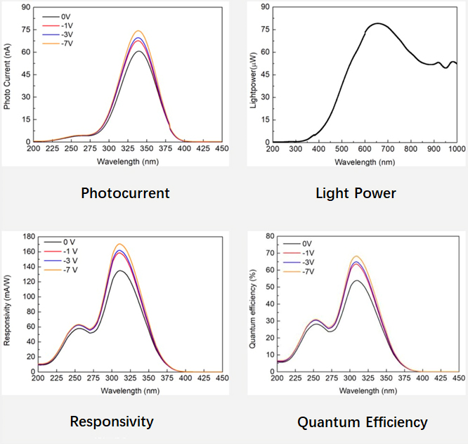
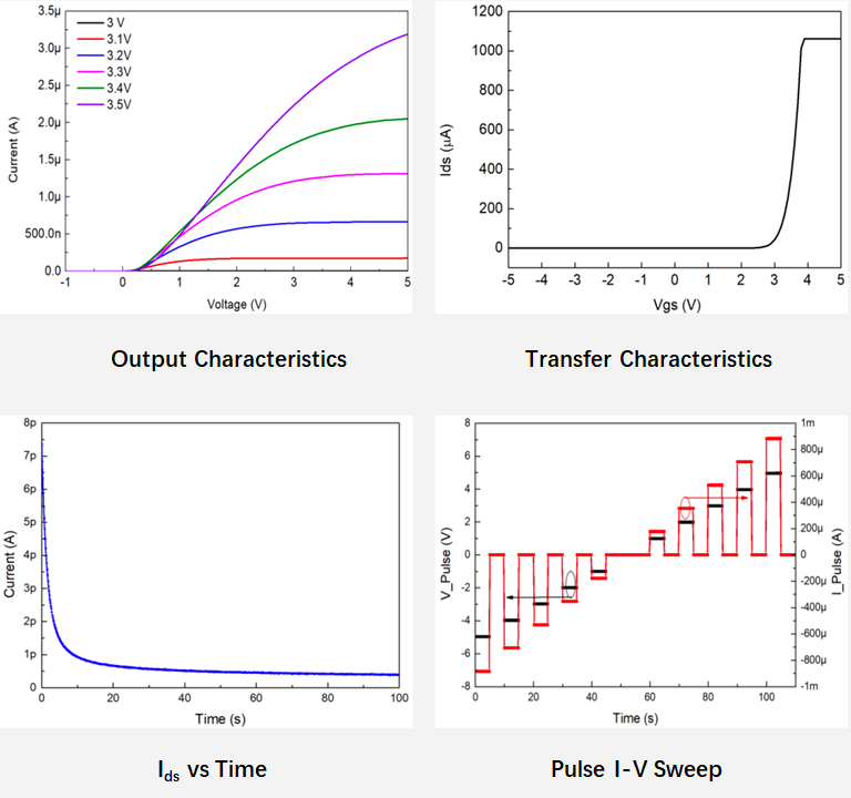
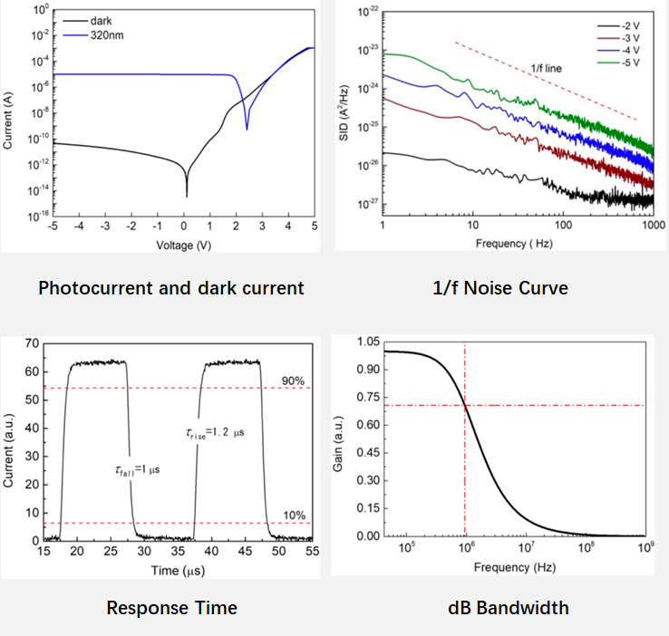
Photodetection Characterization System (OPTOMOS-1000) is a next-generation, all-in-one optoelectronic parameter characterization platform developed for photodetectors and advanced semiconductor devices. Compared with conventional test equipment, it features a more advanced measurement architecture, higher hardware integration, and a more user-friendly software interface—dramatically improving test efficiency and reducing time cost while guaranteeing data accuracy. The system covers a comprehensive suite of measurements: current-voltage (I-V) characteristics, photocurrent spectrum, optical power spectrum, responsivity spectrum, quantum efficiency spectrum, detectivity spectrum, optical response time (3 dB bandwidth), low-frequency / ultra-low-frequency noise spectrum, and transistor transfer/output characteristics. With exceptional functional extensibility, it can be upgraded with a temperature-variable chuck, capacitance-voltage (C-V) scanning, and micro-area photocurrent mapping.
System Photo
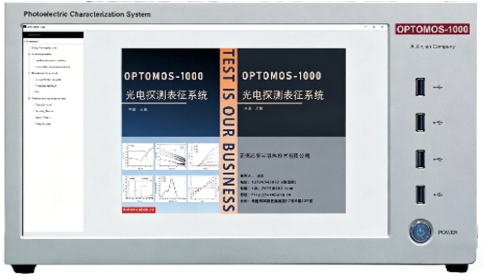
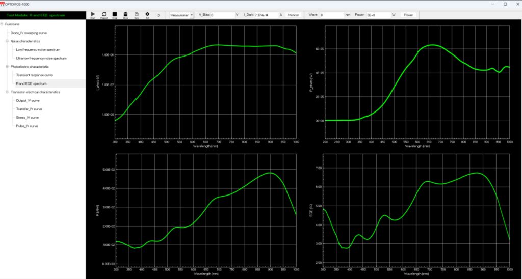
Software Interface
Core Capabilities
- Comprehensive Photodetector Characterization
A single platform covers the full pipeline of photodetector metrology—from DC electrical characteristics (I-V, transfer/output curves) to spectral response (photocurrent, responsivity, EQE, detectivity), time-domain response (3 dB bandwidth), and noise analysis (1/f, RTN, G-R). Replaces multiple standalone instruments with one integrated workstation. - Keithley-4200-Class Current Accuracy
Delivers current measurement precision comparable to the Keithley-4200 SCS. Easily resolves fA-level currents while single-point multi-averaging dramatically reduces jitter in ultra-low-current readings. Minimum EQE detectable: as low as 10⁻⁷ %. - Deep-UV to Near-IR Wavelength Coverage
Equipped with Si and InGaAs standard photodetectors for light-source power calibration, covering the entire deep-UV to near-IR region (200–2500 nm). Supports real-time power calibration and one-click switching between measurement modes. Wavelength resolution: 1 nm. - Ultra-Weak Light Signal Detection
By suppressing system noise to the fA level, the OPTOMOS-1000 captures ultra-weak optical response signals that are inaccessible to conventional lock-in-only systems—precisely quantifying nW-level light signals, responsivity, and quantum efficiency. - Fast Optical Switching & Virtual Oscilloscope
A high-speed current switch module delivers optical rise times < 50 ns, minimizing switching delay artifacts in response-time measurements. The built-in virtual oscilloscope directly displays dynamic current waveforms and auto-calculates 3 dB bandwidth, eliminating external hardware and post-processing overhead. - (Ultra-)Low-Frequency Noise Power Spectral Density
Equipped with ultra-low-noise and high-speed current amplifiers, supporting both broadband low-frequency (1 Hz–1000 kHz) and ultra-low-frequency (0.01 Hz–10 Hz) noise testing. Enhanced electromagnetic shielding achieves a noise floor of 2×10⁻²⁹ A²/Hz @1 Hz or 1×10⁻³¹ A²/Hz @1 Hz, meeting the demands of ultra-low-leakage GaN and Ga₂O₃ devices. - Three-Terminal Transistor Characterization
Full support for three-terminal device electrical testing—transfer and output characteristics, current stress curves, and pulse I-V. Includes low-frequency noise testing for three-terminal devices and bias-stress current-degradation tracking.
Key Specifications
| Item | Specification |
|---|---|
| Bias voltage range | ±10 V |
| Current resolution | < 10 fA |
| Maximum current | 1 mA |
| Monochromator wavelength range | 0–2200 nm |
| Data sampling rate | 2 M/s |
| High-speed current gain | 10³ – 10¹¹ |
| Low-speed current gain | 10⁵ – 10¹⁴ |
| System current noise floor | 10⁻²⁸ A²/Hz, 10⁻³⁰ A²/Hz |
| Low-frequency noise range | 1 Hz – 1000 kHz |
| Ultra-low-frequency noise range | 0.01 Hz – 10 Hz |
| Optical response wavelength | 200 – 2500 nm (Si & InGaAs calibration) |
| Wavelength resolution | 1 nm |
| Xenon light source | 150 W (imported) |
| Optical switch rise time | < 50 ns |
| Max. photocurrent response time | < 100 ns |
| Min. EQE detectable | 10⁻⁷ % |
| Measurement functions | I-V, photocurrent spectrum, optical power spectrum, responsivity, QE, detectivity, 3 dB bandwidth, 1/f noise, transfer/output characteristics, pulse I-V |
| Output formats | BMP (image) + XLS (data), simultaneous |
| Data processing | RMS / Vector / Peak; dynamic averaging up to 500× |
Optional Upgrades
| Module | Specification |
|---|---|
| High-temperature chuck | Room temperature – 200 °C |
| C-V scanning system | 40 V range; up to 2 MHz variable-frequency capacitance & conductance sweep |
| Micro-area photocurrent mapping | 1 μm resolution; DC & lock-in modes; in-situ overlay |
Technical Highlights
- All-in-One Workstation: replaces Keithley sourcemeters, lock-in amplifiers, monochromators, and oscilloscopes in a single integrated platform
- fA-Level Current Resolution: comparable to Keithley-4200 SCS with multi-average jitter suppression
- Deep-UV to Near-IR Coverage: 200–2500 nm with Si/InGaAs calibration detectors
- Ultra-Low Noise Floor: down to 10⁻³¹ A²/Hz @1 Hz for ultra-low-leakage devices
- Sub-50 ns Optical Switching: enables genuine sub-microsecond response-time measurements
- One-Click Auto-Measurement: spectral response, calibration, and data export with a single command
- Dynamic Averaging Visualization: RMS, Vector, Peak modes with up to 500× averaging
- Bad-Point Removal: online outlier deletion for cleaner, more reliable curves
- Modular Expandability: temperature-variable chuck, C-V scanning, and 1 μm-resolution photocurrent mapping available as upgrades
Typical Applications
- Photodetector Spectral Response: photocurrent, responsivity, quantum efficiency (EQE), and detectivity spectra from deep-UV to near-IR
- Ultra-Weak Light Detection: nW-level optical signal capture, minimum EQE down to 10⁻⁷ %
- Photodetector Response Time: 3 dB bandwidth, sub-microsecond photocurrent response, virtual oscilloscope time-domain analysis
- Low-Frequency Noise Analysis: 1/f, RTN, G-R noise for defect and trap-state studies
- Image Sensors & Focal Plane Arrays: pixel-level characterization, dark current mapping
- Wide-Bandgap Semiconductors: GaN, Ga₂O₃, and other ultra-low-leakage devices
- Transistor Electrical Characterization: transfer/output curves, pulse I-V, bias-stress degradation tracking
- Perovskite & 2D Photodetectors: charge-injection effects, photo-bias stability
- Infrared & SWIR Detectors: InGaAs-based near-IR and short-wave infrared characterization
- Quantum Dots & Nanowire Photodetectors: spectral response and noise performance
Results Display