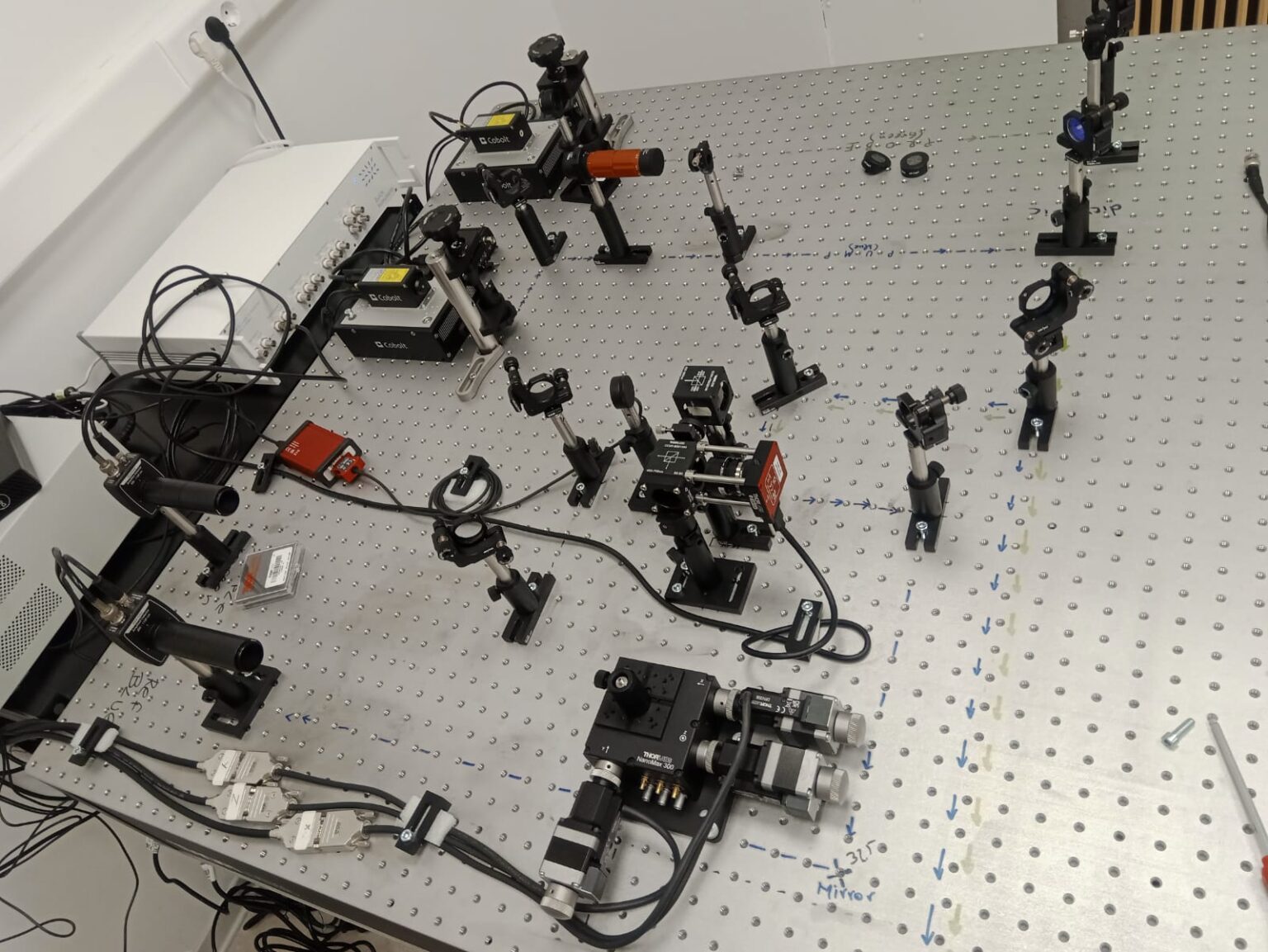

FDTR Thermal Conductivity Measurement System, developed by Metathermo (Suzhou) Energy Technology Co., Ltd., is a non-contact, micro/nanoscale thermophysical property characterization platform based on the photothermal detection principle. Using two laser beams (pump + probe) to excite and detect periodic temperature oscillations on a metal transducer/sample surface, the system extracts thermoreflectance variations with modulation frequency to inversely determine thermal conductivity, thermal diffusivity, and interfacial thermal resistance. Covering thin films, bulk materials, and micro/nanoscale heterostructures, it serves thermal management materials, 2D electronic devices, thermoelectric materials, and low-dimensional physics research.
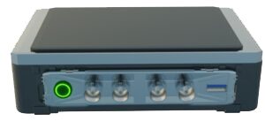
Metathermo 3-Omega Thermal Conductivity Measurement System is based on the classic 3ω harmonic electrothermal detection technique. By applying an ω-frequency AC current through a microfabricated metal line, it generates 2ω Joule heating and extracts the 3ω voltage signal to inversely determine thermal conductivity. Designed for solids, liquids, fluids, thin films, and irregular surfaces, the compact desktop system has been adopted by multiple laboratories in Europe and North America, serving research in materials science, chip thermal management, thermoelectric materials, and nanofluids.
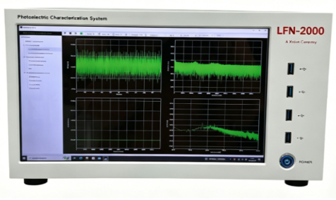
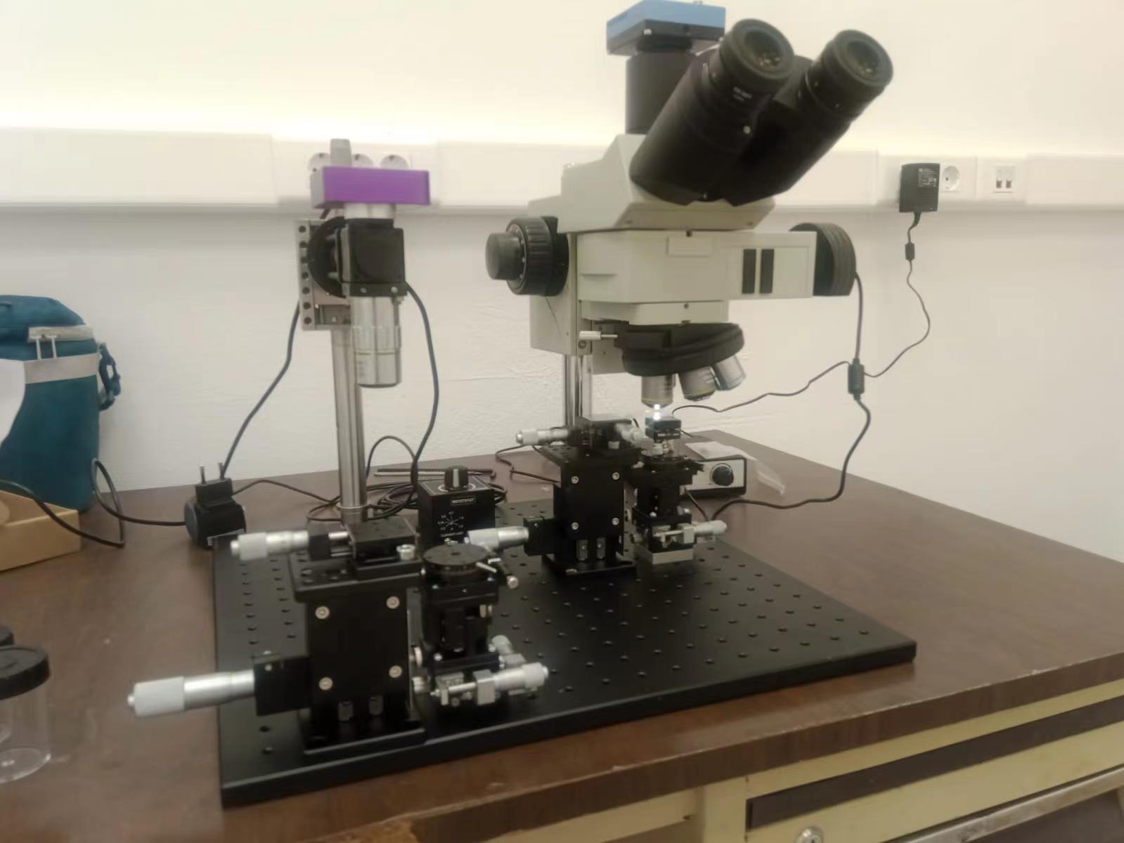
LFN-2000 is a cost-effective test system integrating low-frequency and ultra-low-frequency noise measurement, IV/IT curve sweeping, and pulsed voltage/current readback. Its compact structure incorporates a miniature optical platform, low-noise current amplifier, spectrum analyzer, and optical microscope. Core modules from leading international brands ensure high measurement accuracy. When coupled with a probe station and shielding enclosure, the system achieves a current noise floor of 2×10⁻²⁹ A²/Hz, with ultra-low-frequency noise below 2×10⁻³¹ A²/Hz. Supporting both two-terminal and three-terminal testing, it meets a wide range of characterization requirements.
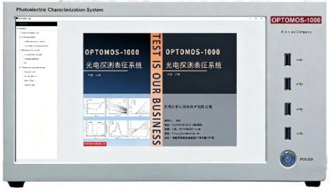
OPTOMOS-1000 is a next-generation photodetection characterization system. Compared with conventional setups, it offers advanced measurement schemes, higher integration, and user-friendly software for efficient, accurate testing. The platform measures I-V curves, responsivity, quantum efficiency, detectivity, 3 dB bandwidth, (ultra-)low-frequency noise, and transistor characteristics. Hardware includes an optical platform, xenon source, monochromator, microscope, amplifiers, and data acquisition. Upgradable with temperature-variable chucks, C-V scanning, and micro-area photocurrent mapping, it serves 2D materials, infrared detectors, single-photon devices, and advanced photodetector arrays.
The 2D Material Transfer Platform is a high-precision modular system designed for deterministic transfer of two-dimensional (2D) materials and van der Waals (vdW) heterostructure assembly. It supports precise pick-up and placement of graphene, transition metal dichalcogenides (TMDCs, e.g., MoS₂, WSe₂), hexagonal boron nitride (hBN), and other layered crystals, making it suitable for frontier fundamental research laboratories and small-batch device fabrication. With sub-micron alignment accuracy and clean, residue-free interfacial contact, the system is an ideal tool for constructing twistronics devices, optoelectronic devices, and quantum devices.
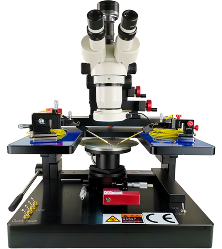
Metathermo’s PIP Series Manual Probe Stations are precision benchtop platforms for on-wafer electrical characterization of semiconductor devices, materials, and packages. Covering 4-inch (Mini), 6-inch (Compact), 8-inch (Mid-size), and 12-inch (Large) configurations, the series supports I-V/C-V testing, RF probing, and high-frequency measurements across R&D, failure analysis, and small-batch production. With modular microscope units, magnetic probe bases, vacuum chucks, optional heating stages (up to 500 °C), pneumatic controls, and HD industrial cameras, the PIP series bridges fundamental device evaluation and practical wafer-level testing.
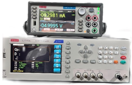
Semiconductor Parameter Test System (SPA) is a cost-effective platform adopting the Kelvin four-wire method, integrating an auto-balancing high-precision LCR meter and a Keithley 2450 Source Measure Unit (SMU). It performs two-terminal I-V sweeping and current/voltage stress, three-terminal transfer and output characteristics, and frequency-dependent C-V measurements. Designed to match the capabilities of the Keithley 4200A-SCS, it delivers high-precision semiconductor device characterization at a competitive price.