
Magnetron Sputtering System
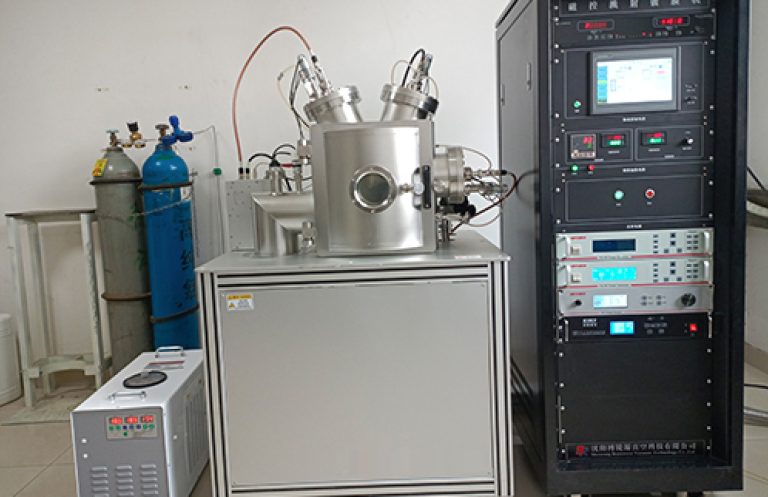
Magnetron Sputtering System is a high-vacuum physical vapor deposition (PVD) platform designed for universities, research institutes, and pilot-scale material development. Built around a 316 stainless steel vacuum chamber, the system supports single target, multi-target, and co-sputtering configurations for metals, alloys, dielectrics, doped films, and multilayer stacks. It is well suited to semiconductor materials, 2D materials, optoelectronics, energy-storage electrodes, and functional coating research.
Product Image
Core Capabilities
- High-Vacuum 316 Stainless Steel Chamber
The Φ400 × 450 mm chamber is made of 316 stainless steel, with 304 stainless steel top/bottom plates, an omnidirectional viewport with shutter, and standard CF/KF vacuum flanges. The design ensures low leak rate, bakeability, and easy maintenance for high-frequency daily use. - Multi-Target Magnetron Architecture
Supports 1–4 inch sputter targets with 2–4 target positions. DC power is used for metals and conductive targets; RF power handles oxides, ceramics, and other insulating targets. Single-layer, multilayer, alloy co-sputtering, and reactive sputtering (with O₂/N₂ process gases) are all supported. - High-Temperature, Uniform Sample Stage
The stage accepts 1–4 inch substrates with adjustable rotation from 0–20 rpm to improve thickness uniformity. Maximum heating temperature is 800 °C, with Japanese conductivity-meter PID control and ±0.5 °C accuracy—ideal for oxide films, high-temperature nucleation, and stress engineering. - Clean Deposition Environment
A mechanical pump plus turbo-molecular pump combination reaches an ultimate vacuum of 5×10⁻⁵ Pa. Combined ionization/resistance gauges monitor chamber pressure, reducing residual-gas contamination for sensitive films such as semiconductors, superconductors, and 2D-material interface layers. - Customizable and Service-Friendly
Water-cooled cathodes, electrically lifted top cover or front-opening door, and expandable gas/power/stage options make the system adaptable to specific projects. On-site installation, commissioning, and training are included, with a 2-year warranty—well suited to small labs without dedicated vacuum engineers.
Technical Specifications
| Item | Specification |
|---|---|
| Chamber Material and Size | 316 stainless steel; top/bottom plates 304 stainless steel; Φ400 × 450 mm |
| Viewport | Omnidirectional view, with shutter |
| Chamber Opening | Motorized top-cover lift / front door |
| Sample Stage | 1–4 inch substrates; rotation 0–20 rpm adjustable |
| Heating Temperature | ≤800 °C, PID control, accuracy ±0.5 °C |
| Sputter Targets | 1–4 inch; 2–4 target positions optional; water-cooled cathode |
| Power Supply | DC 500 W; RF power optional; bias cleaning 500 V |
| Vacuum System | Mechanical pump + turbo-molecular pump; 8 L/s mech. pump, 1200 L/s turbo pump |
| Ultimate Vacuum | 5×10⁻⁵ Pa |
| Vacuum Measurement | Ionization gauge + Pirani/resistance gauge |
| Flange Interfaces | Pumping CF150/CF200, exhaust KF25, gas inlet φ6 ferrule |
| Gas Lines | Ar/O₂/N₂ etc., MFC control (optional/custom) |
| Dimensions | 700 × 820 × 870 mm |
| Weight | Approx. 200 kg |
Typical Applications
- Semiconductors & Microelectronics: metal electrodes, barrier layers, seed layers, ITO/IZO transparent conductive films
- Advanced Materials: alloy films, high-entropy alloys, doped oxides, reactive sputtered nitrides
- 2D Materials & Devices: contact electrodes, encapsulation metal layers, graphene/hBN device interconnects
- Energy Storage: current-collector coatings, solid-electrolyte buffer layers, catalytic electrode films
- Optical & Functional Coatings: anti-reflection coatings, reflective films, hard wear-resistant coatings, decorative films